Skip to end of metadata
Go to start of metadata
Big version features
Project Notes
Components:

Schematic:
Layout:
Requested Changes by Austin
Both boards:
V1
Remove resistors on IMU (the two resistors are only put there is we are trying to configure the board into I2C mode, but we are using the default SPI mode for which the resistors should not be connected)
Easy way to tie GPIO 1 to GPIO 8 and a way to tie GPIO1 to GPIO9 with pin header. This is useful for lighthouse localization.
There is a discrepancy between the bond diagram for ALWAYSON_LDO_OUT for https://github.com/PisterLab/scum-dev-board/blob/quikpak_ll/qfn_info/bigBoard_bond_diagram.pdf and https://github.com/PisterLab/scum-dev-board/blob/master/scum3c_devboard_large/Images/scum3C%20Large%20Board%20bond%20diagram.png . Both boards have this discrepancy and should be modified to match the first link.
Add the missing SCuM pins to schematic (mark as no connections) just for bookkeeping
Currently SDO pin on IMU is connected to GPIO12 and SDI pin on IMU is connected to GPIO13. It would be nice to have SDO pin on IMU connected to GPIO13 instead and SDI pin of IMU connected to GPIO12. This is to match the hardware configuration with the code Brian wrote before to maintain as much consistency between boards as possible so code can be reused across all of them.
Request from DB: “it would be nice to have plated vias on as many of the SCuM pins as possible so we can fully wirebond and then thread a 30 AWG wire in if we need to splice something on“
McCoy (small) board:
Pin layout: https://docs.google.com/drawings/d/1l1O0RtISmslJsic9txYNfCFIynfG-745T3hjRpNIH5w/edit?usp=sharing
V1
First round review:
Pin layout updates
Need hard reset for 3wb programming. The pins on the board should be ordered: hard reset, clk pin, enable pin, data pin
Put pins of IMU VDDIO and IMU VDD directly next to VDDIO pins so we can easily tie both of those pins to VDDIO (when using the IMU, VDDIO will be 1.8V, which is what we need for IMU VDDIO and IMU VDD)
Pin header to easily tie VBAT to VDDIO
Would be nice to have a VDDD pin directly next to boot source select pin, so they can be tied together with a header (this is done to enable 3wb programming rather than optical programming)
Use 2.54 mm (standard size) pin headers instead of 1.27mm.
“IMU” pin and trace don’t need to be present since that is used to put the IMU in I2C mode, but we don’t use that (we use SPI mode for the IMU)
Modifications to the surface mount components as annotated here: https://github.com/PisterLab/scum-dev-board/blob/master/scum3c_devboard_deleted_elements/pictures/scum3c-devboard_schematic_Page_2%20annotated.jpg
GPIO11 should have a pin (it currently doesn’t)
Would be nice, but not necessary for GPO_ZERO to have a pin output
Second round review (Modifications discussed on 4/14/21 SCuM meeting)
Instead of having GPIO1 on a separate header integrate it into the same header as the GPIO (still allowing GPIO1 to be tied to GPIO8 to GPIO9)
Align right side header of board with nRF pins (https://www.nordicsemi.com/Software-and-tools/Development-Kits/nRF5340-DK ). Pins are configurable on nRF and to make a ground we could just hold a GPIO output on the nRF low.
We should consolidate pins on the board (right now there are a number of separate headers).
The GPIO1 pins that are going to be tied to GPIO8 and GPIO9 should be directly next to each other so that we can really easily tie them together with a pin jumper header. We proposed adding another column of GPIO1 pins (still 2 rows) to the GPIO header (remove one of the ground columns) so that we can accomplish that.
Additional comments
Anyway we could shrink back down the dimensions of the board? Seems like there is some empty space in parts of the board that we could compress down to make the board smaller.
4/27/21 Review
Add nRF pin labels
Move antenna back to separate pin
Minor revisions to the proposed pin layout
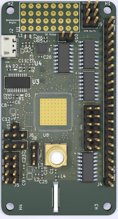
Spock (large) board:
Pin layout: https://docs.google.com/drawings/d/1-NSjz1xg-1bFSp3lY8e1M7UuoZM1Tlf1_K2JZVS5FTk/edit?usp=sharing
V1
First round review
IMU
Remove I2C pull-up selector for IMU
Board labels
Labels are hard to read, make them bigger
Label IMU orientation on PCB
Would be nice to have GPIO numbers on the GPIO header
Labels on the board for the teensy row would be nice (at least for GPIOs)
Antenna
Let’s go with the through hole antenna connector rather than the one that is flush with the board
Voltage sources
Need places to measure current along VBAT, VDDIO, and VDDD path (this would be just a break in the trace with two pin headers exposed to easily measure current along the path). When not measuring we would just have a jumper header there.
Would be nice to have VIN pin on the bottom left header along with with other source voltages that are already there (VBAT, VDDD, VDDIO) + put another GND pin next to it
Schematic
PIN numbers on schematic for Teensy don’t actually match the pin numbers/labels on teensy itself. It would be nice to have them match
Level shifters
U4 has direction grounded, when in reality the direction should be set to VDDIO since RsTx is an output on SCuM and that output needs to be raised to VIN before it goes to Teensy or to USB UART
Misc
Make sure issues with Vin trace and VDDD trace missing are no longer problems when we export to Gerber files again
ADC input and ADC_LDO_OUTPUT should each go to a pin header so that we can access it
Second round review
Make sure VDDIO, VBAT, VDDD selection headers can be used to measure just the respective currents going into SCuM (not measuring current going to the external components)
Change UART label on VIN to say USB instead
Remove option to set VDDD to VBAT
For vias on board that will be probed, make sure they don’t have the solder mask in them so that they have metal that we can directly probe
AC couple GND from USB cable to ground for UART setup?? (not sure exactly what Brad was saying. Same trace length on UART setup? (also not entirely sure what Brad was saying). Follow guidelines: https://www.ftdichip.com/Support/Documents/AppNotes/AN_146_USB_Hardware_Design_Guidelines_for_FTDI_ICs.pdf
Clarification from DB (ask DB if questions): Connect the USB connector shield to GND via a surface mount passive. Sounds like there are clear advantages to being able to isolate the DC level of the board from the DC level of the PC, so that surface mount passive might need to be a capacitor. 2) Treat the D+ and D- pins from USB as sensitive traces and do all the stuff you would do with a sensitive trace: no sharp corners, no vias, make them the same length, etc. Strong recommend to do exactly what FDTI advises in the app note 146 PDF or else USB is just going to work badly.
GND pin alongside the ADC input pin
DB: There are a few unconnected nets when I run layout DRC (besides the ones in the ground pad under SCuM)
Consider a USB connector with through-hole chassis pins to keep it from ripping off
We should have regulators to level shift the VDDIO SCuM output signals from GPIO12,14,15 down to the 1.8V source so that we can operate VDDIO at Vin=3.3V, but then communicate with the IMU at the lower 1.8V that matches IMU VDDIO. GPIO13 is an output from IMU into SCuM input, so this will need to be level shifted from IMU VDDIO = 1.8V up to VDDIO. NOTE: The GPIO numbering I list here is assuming that you have made the modification I suggested in the “Both boards“ section about flipping GPIO12 and GPIO13
Third round review (Requests from SCuM meeting 4/14/21)
Can we try to consolidate some of the pin headers on the board into a small number of headers (same number of pins), so there aren’t as many connectors that need to be soldered to the board. Although ADC input/output should be near development region.
NOTE: New proposed layout still has weird pin header shapes. Would be nice to have a big 2 by X header that fits a lot of the pins rather than having the width of the header be 3 in some places. Same with GPIO pin header it would be nice to have the max width be 2.
The GPIO1 pins that are going to be tied to GPIO8 and GPIO9 should be directly next to each other so that we can really easily tie them together with a pin jumper header
Let’s try and rearrange Teensy pins so that we could also plug in headers going into an nRF board. Here is the nRF board for reference: https://www.nordicsemi.com/Software-and-tools/Development-Kits/nRF5340-DK . SEE DB’s PROPOSED TEENSY PIN LAYOUT FROM HIS EMAIL.
Remove VDDD select (we will never set VDDD to VBAT), but still make sure that we have a pin header to tie VDDD to 1V source (sometimes we might want to provide external VDDD and also having a pin header to select this will let us measure VDDD current if we want).
Add breaks in the trace for IMU VDDD and IMU VDDIO so we can put a headers down if we want to power the IMU and remove the headers if we don’t want to power the IMU
It would be nice to have all pins of Teensy on the header (currently the two pins after 3.3V from Teensy are not included). We could just not route those pins anywhere on the board, but it would be nice so there are no questions about how to plug in the Teensy. (this isn’t super important if this is difficult)
Additional requests:
There should be an option to cut power going to IMU. We should put a pin header along the trace going into IMU VDD and IMU VDDIO so we can cut power to the IMU by removing a header and also have the ability to measure the current that the IMU is consuming.
To discuss:
Radio performance on both of the working big boards has been pretty bad…. A lot of packets are received when doing a sweep, but most of the packets have corruption in the data, which is unexpected since the same code results in properly received packets when I use my cold boot SCuM dev board.
V2
Realized I messed up the ASC pin layout for Teensy since some of the pins on Teensy don’t have digital output… this isn’t a dealbreaker since writing to ASC can be done on software side of SCuM. If we do another iteration then fix this otherwise not a big deal
Labels near edge of board for IMU are too close to pin header so they get covered by the pin header. Would also be nice to have those labels slightly larger since they are hard to read
Many of the labels for the GPIOs on the side with GPIO15 are covered by vias and thus unreadable
VDD on top right of SCuM isn’t connected to the other VDD trace on the top of the board. It should be.
Notes for those assembling boards
Small board
Big board
For first iteration on board, don’t put R5 and R6 since we don’t want IMU in I2C mode
Don’t put C1 and L4 since we don’t want to use the chip antenna (at least not yet). Additionally the chip antenna shouldn’t be added.
The through hole antenna will be solder on after the surface mount components (Austin will do this)
We moved to through hole USB port. This should still be soldered on with the solder paste and then I (Austin) can solder the final connections.
The USB port has a new capacitor on it that doesn’t have a label…. I believe 0.1uF should be fine to put there